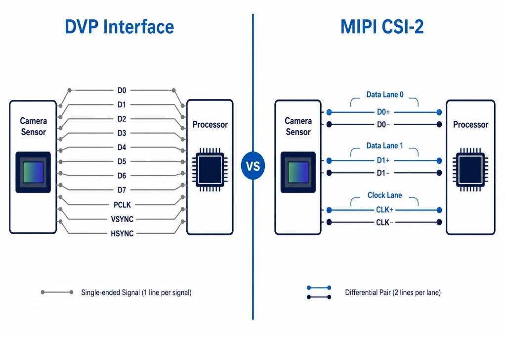
DVP (Digital Video Port) is a parallel camera interface that transmits pixel data across 8–14 data lines simultaneously, making it simple to integrate with MCUs but limiting bandwidth to approximately 720p at 30 fps in practice. MIPI CSI-2 is a serial differential interface that delivers up to 2.5 Gbps per lane — supporting 4K and beyond — in a 4–6 wire connection that consumes less power, generates less EMI, and routes cleanly on compact FPC flex cables. Choosing the wrong interface for your host platform is one of the most common and most expensive embedded camera design mistakes.
Key Takeaways
- DVP is parallel: 8–14 data lines + PCLK + VSYNC + HSYNC = 12–18 total signals. Simple bring-up, no high-speed PCB rules, natively supported by STM32 DCMI and many MCU camera peripherals.
- MIPI CSI-2 is serial: 1 clock pair + 1–4 data lane pairs = 4–10 total differential signals. Up to 2.5 Gbps/lane (D-PHY), supports 1080p through 8K, standard on all modern ARM SoCs.
- Bandwidth ceiling: DVP practical maximum ≈ 720p @ 30 fps with 8-bit bus at 72 MHz PCLK. MIPI 2-lane @ 1.5 Gbps/lane = 3 Gbps — sufficient for 4K @ 30 fps RAW10.
- Cable length: DVP parallel traces degrade beyond 10–15 cm due to skew. MIPI FPC standard length is ≤30 cm; extensions require a repeater/retimer chip.
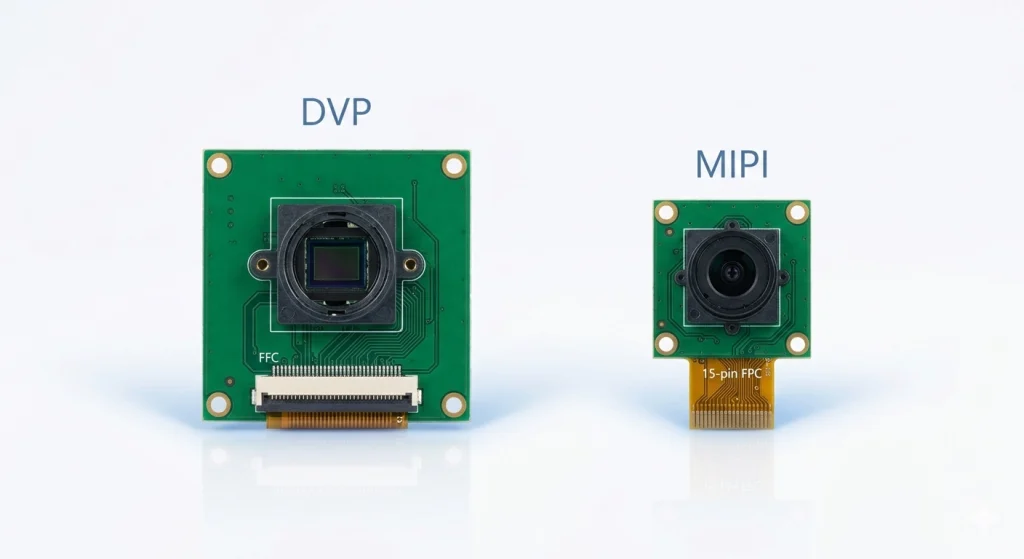
- Smeiker supplies camera modules in both DVP and MIPI interfaces, with custom FPC length and connector options for OEM integration.
DVP Interface: How the Parallel Camera Standard Works
DVP — Digital Video Port — is the legacy parallel camera interface that dominated embedded camera design through the mid-2010s and remains relevant today in MCU-based and cost-sensitive embedded systems. Its operating principle mirrors that of a classic digital bus: each bit of each pixel's data has its own dedicated wire, and all bits arrive simultaneously at the receiver on each rising (or falling) edge of the pixel clock (PCLK).
DVP Signal Structure
A standard 8-bit DVP connection requires the following signals from sensor to host:
- D[7:0] — 8 data lines, carrying one byte (one pixel component) per PCLK edge. Some sensors support 10-bit or 12-bit DVP, adding 2 or 4 more data lines.
- PCLK — Pixel Clock. Driven by the sensor. The host latches data on each PCLK edge. Typical frequencies: 12–96 MHz (practical maximum ~72 MHz for reliable parallel operation on most MCUs).
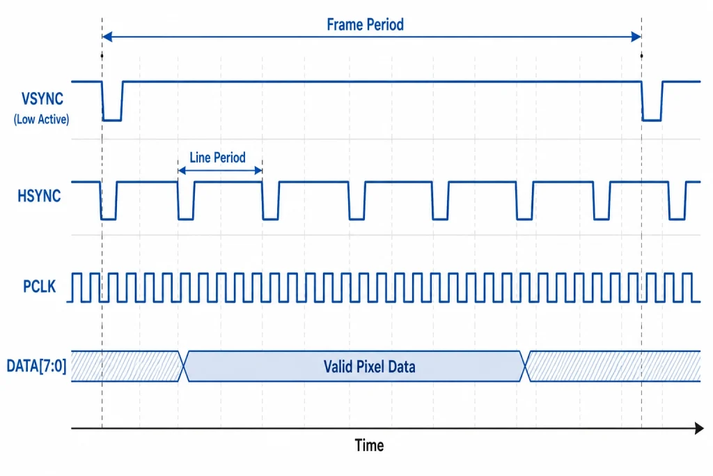
- VSYNC — Vertical Sync. Pulses once per frame, marking the start/end of each image frame. At 30 fps, VSYNC toggles at 30 Hz.
- HSYNC / HREF — Horizontal Sync. Pulses once per line, marking valid pixel data rows. At 30 fps with 480 lines, HREF toggles at 14,400 Hz.
- XCLK — Master Clock Input to the sensor (host-provided, typically 6–27 MHz). The sensor's internal PLL derives PCLK from XCLK.
- SCCB / I²C — Serial Camera Configuration Bus. A separate 2-wire interface for writing ISP register settings (exposure, gain, resolution, format).
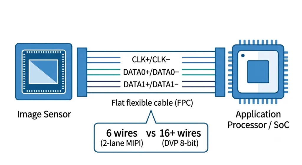
Total signal count for an 8-bit DVP module: 8 (data) + 4 (PCLK, VSYNC, HSYNC, XCLK) + 2 (I²C) + 2 (power) = 16 pins minimum. A 10-bit bus requires 18 pins; 12-bit requires 20. This pin count directly translates to connector size and PCB routing complexity. STMicroelectronics' DCMI application note AN5020 provides the canonical reference for interfacing DVP sensors with STM32 MCUs, covering timing requirements, DMA transfer, and compatible sensor list.
DVP Bandwidth: The Practical Ceiling
DVP bandwidth is calculated as: Data Rate = PCLK × bit depth × 1 pixel per clock. At a practical PCLK maximum of 72 MHz with an 8-bit bus:
- Raw data rate: 72 MHz × 8 bits = 576 Mbps (72 MB/s)
- At YUV422 (2 bytes per pixel): ~36 megapixels/second → covers 720p @ 30 fps (921,600 pixels/frame × 30 × 2 bytes = 55 MB/s ✅)
- 1080p @ 30 fps (6.2 MB/frame × 30 = 186 MB/s) exceeds the practical DVP ceiling unless JPEG compression is applied in-sensor before the bus.
This is why sensors above ~3MP almost universally offer MIPI as their primary interface: DVP simply cannot move the data fast enough for uncompressed high-resolution output. The OmniVision OV2640 (2MP) and OV7670 (VGA) — two of the most widely deployed DVP sensors in MCU projects — operate comfortably within this ceiling. The OV5640 (5MP) technically offers a DVP mode but requires either reduced resolution or in-sensor JPEG compression to stay within bus limits.
DVP Signal Integrity Constraints
Parallel buses introduce a fundamental PCB design challenge: skew. All 8–12 data lines must arrive at the receiver within a fraction of a PCLK cycle — at 72 MHz, the setup/hold window is ~7 ns. Length-matching all data traces to within ±5 mm is standard practice, and the entire bus must be routed away from high-frequency switching nodes to avoid coupling noise. Beyond 15 cm of trace length, parasitic capacitance degrades edge rates enough to require series termination resistors, adding BOM cost and tuning effort. This is why DVP modules on rigid PCBs are straightforward, but DVP over flex cables longer than 10–15 cm is rarely attempted in production designs.
Factory Perspective — DVP Skew Failure in Production: "A customer brought us a thermal imaging module they had designed using a DVP-interface LWIR sensor on a 20 cm flex cable connecting to an STM32H743 MCU. In lab testing on a short bench harness the image was clean; on the production unit with the full cable routed around the enclosure, every unit showed intermittent horizontal line corruption — 3–6 pixel-wide horizontal bands appearing randomly, especially after thermal cycling. The root cause was PCLK-to-DATA skew on the flex cable: the PCLK trace was 18 mm shorter than the D7 and D6 lines (routed around a cutout), pushing skew to 120 ps — outside the sensor's 70 ps setup spec at 50 MHz. We redesigned the FPC layout with matched-length trace routing (±3 mm), added 22 Ω series termination on PCLK and all data lines, and reduced the operating PCLK from 50 MHz to 36 MHz to widen the timing margin. Line corruption dropped to zero across 200 production units in the final reliability run. The lesson: DVP is deceptively simple at the register level but unforgiving on PCB/FPC layout at frequencies above 30 MHz." — Smeiker Hardware Engineering Team
MIPI CSI-2 Interface: How the Serial Differential Standard Works
MIPI CSI-2 (Camera Serial Interface version 2), maintained by the MIPI Alliance, is the dominant camera interface standard for all modern ARM-based SoCs — including Rockchip, Qualcomm, MediaTek, NXP i.MX, NVIDIA Jetson, Raspberry Pi CM4/5, and virtually every mobile application processor released since 2010. Unlike DVP's wide parallel bus, MIPI CSI-2 transmits all data over one or more high-speed differential lane pairs — two wires per lane, one carrying the signal and one its inverse, eliminating common-mode noise at the receiver.
MIPI CSI-2 Signal Structure
A 2-lane MIPI CSI-2 connection — the most common configuration for 1080p–4K embedded cameras — requires:
- CLK+ / CLK− — 1 differential clock lane pair (2 wires). Carries the high-speed bit clock derived from the lane data rate.
- DATA0+ / DATA0− — Lane 0 differential data pair (2 wires).
- DATA1+ / DATA1− — Lane 1 differential data pair (2 wires). Total: 6 signal wires for a 2-lane interface.
- I²C / CCI — Camera Control Interface, a 2-wire I²C-compatible bus for sensor register access. Separate from the high-speed data path.
- RESET / PWDN — GPIO-level control signals for power management.
The total FPC connector pin count for a standard MIPI module is typically 15–24 pins (including power rails and I²C) — far fewer than a DVP equivalent at the same or higher resolution, which enables smaller connectors (0.5 mm pitch FPC vs. 1.0 mm pitch ZIF) and narrower flex cables.
MIPI CSI-2 Bandwidth: Lane Count and Speed
MIPI D-PHY (the most common physical layer for CSI-2 in embedded systems) supports up to 2.5 Gbps per lane at D-PHY v2.0. In practice, most embedded SoCs support 1.0–1.5 Gbps per lane. Bandwidth scales linearly with lane count:
| Lane Config | Speed per Lane | Total Bandwidth | Max Practical Resolution |
|---|---|---|---|
| 1-lane | 1.0 Gbps | 1.0 Gbps | 720p @ 60 fps RAW8 |
| 2-lane | 1.5 Gbps | 3.0 Gbps | 1080p @ 60 fps RAW10 / 4K @ 15 fps |
| 4-lane | 1.5 Gbps | 6.0 Gbps | 4K @ 30 fps RAW10 / 1080p @ 120 fps |
| 4-lane | 2.5 Gbps | 10.0 Gbps | 8K @ 30 fps / 4K @ 120 fps |
MIPI CSI-2 Cable Length: The FPC Constraint
MIPI CSI-2 D-PHY is specified for short-reach board-to-board connections. Standard FPC cable implementations are reliable up to 20–30 cm depending on lane speed and FPC impedance. Beyond 30 cm, differential pair skew, insertion loss, and reflections at impedance discontinuities (connector transitions) degrade eye diagrams below the D-PHY receiver mask. Solutions for longer distances include:
- MIPI retimer / repeater ICs (e.g., Texas Instruments SN75DPHY440SS): re-drive the D-PHY signal, extending reach to ~50–80 cm. Adds BOM cost (~$2–5/unit) and one design revision cycle.
- MIPI A-PHY SerDes: the MIPI Alliance's long-reach physical layer, supporting up to 15 m over coax/STP — used in automotive ADAS and remote-camera industrial systems, but requiring specialized deserializer ICs at the SoC end.
- FPD-Link III / GMSL2: competing automotive-grade SerDes standards from TI and Analog Devices, supporting 10–15 m cable runs, widely deployed in robotics and surveillance camera systems with remote sensors.
For the vast majority of embedded product designs — kiosks, AGVs, drones, smart terminals — the camera module and host SoC are within 30 cm of each other, and standard MIPI FPC is the correct choice. Smeiker's MIPI camera modules are available with standard 15 cm FPC and custom lengths up to 30 cm; longer-reach options with retimer are available as ODM configurations.
DVP vs MIPI CSI-2: Complete Specification Comparison
The following table covers every engineering-relevant parameter for hardware engineers selecting a camera interface for a new embedded system design or evaluating a module upgrade.
| Parameter | DVP (Parallel) | MIPI CSI-2 (Serial) |
|---|---|---|
| Signal Type | Single-ended parallel | Differential serial (LVDS) |
| Data Width | 8 / 10 / 12 / 14 bits parallel | 1 / 2 / 4 serial lanes |
| Signal Wire Count | 14–20 (incl. clocks + sync) | 4 (1-lane) – 10 (4-lane) |
| Max Practical Bandwidth | ~576 Mbps (8-bit @ 72 MHz) | Up to 10 Gbps (4-lane @ 2.5 Gbps) |
| Max Practical Resolution | 720p @ 30 fps uncompressed; 1080p w/ JPEG | 4K @ 30 fps (2-lane), 8K+ (4-lane) |
| PCB Routing Complexity | Medium — length-matching all data lines required | High — differential pair impedance control (85–100 Ω) |
| FPC / Cable Length | ≤15 cm recommended | ≤30 cm standard; ≤80 cm with retimer |
| EMI Susceptibility | Higher — wide parallel bus acts as antenna array | Lower — differential pairs cancel common-mode noise |
| Power Consumption | Higher I/O switching (many lines toggling at PCLK) | Lower — fewer lines, D-PHY LP/HS power states |
| Driver / BSP Complexity | Low — DCMI peripheral + DMA, minimal driver code | Medium — V4L2 / libcamera driver, D-PHY init sequence |
| Host Platform Availability | STM32 (DCMI), ESP32, AVR (bit-bang), FPGA | All ARM SoCs: Rockchip, RPi, Jetson, NXP, Qualcomm |
| Sensor Availability (>3MP) | Very limited — most ≥5MP sensors drop DVP support | Full range — virtually all modern sensors support MIPI |
| Best Application Fit | MCU-based IoT, barcode scan, low-res machine vision | SBC/SoC platforms, face recognition, AGV, drone, kiosk |
Host Platform Compatibility: Which Interface Is on Your Board?
The single most important factor in camera interface selection is not bandwidth or resolution — it is what interface your target host platform physically supports. Choosing a MIPI camera for an STM32F4-based design adds a bridge chip, a driver porting project, and 6–8 weeks of firmware work. Choosing a DVP camera for a Rockchip RK3568 SBC adds hardware workarounds for a peripheral that simply isn't present. Check your SoC or MCU datasheet first.
Platforms with DVP (Parallel DCMI) Support
- STM32 MCU family — STM32F4, STM32F7, STM32H7, STM32MP1 all include an ST DCMI (Digital Camera and Media Interface) peripheral. 8/10/12/14-bit parallel, up to 50 MHz PCLK on most variants. The canonical reference is ST AN5020. Compatible sensors: OV7670, OV2640, OV5640 (DVP mode), HM01B0.
- ESP32 / ESP32-S2 / ESP32-S3 — All include a hardware camera interface (called DVP in Espressif documentation), supporting 8-bit parallel at up to 40 MHz PCLK. The ESP32-CAM module is the canonical low-cost DVP implementation. OV2640 is the standard paired sensor.
- FPGA-based platforms — DVP is trivially implemented in FPGA fabric via I/O primitives. Suitable for custom machine vision systems where FPGA-side ISP processing is desired.
- Low-cost ARM MCUs with camera peripherals — GD32, AT32, and other STM32-compatible MCUs with DCMI-equivalent peripherals also support DVP.
Platforms with MIPI CSI-2 Support
- Rockchip RK3568 / RK3588 / RV1126 — All include 2–4 MIPI CSI-2 ports with integrated ISP. The Rockchip ISP pipeline (IQ-tuning based) handles RAW sensor data directly from the MIPI receiver. Standard in AIoT, NVR, and edge AI applications. Smeiker's MIPI camera modules are validated on RK3568 and RK3588 platforms.
- Raspberry Pi CM4 / Pi 5 — Dual CSI-2 ports on CM4; Pi 5 adds a second CSI-2 connector. Compatible with standard 15-pin / 22-pin FPC MIPI modules via V4L2 / libcamera stack. Most widely used development platform for MIPI camera bring-up.
- NVIDIA Jetson Nano / Orin NX / AGX Orin — 2–6 MIPI CSI-2 ports depending on module. ISP handled by Jetson's built-in ISP or bypassed to CUDA for custom processing. Standard for edge AI and robotics camera integration.
- NXP i.MX8M / i.MX93 — 2–4 MIPI CSI-2 lanes per port. Used in industrial HMI, medical devices, and automotive infotainment. Supports ISP-less and ISP-enabled pipeline configurations.
- Qualcomm Snapdragon (embedded variants) — Multiple MIPI CSI-2 ports, typically used with proprietary camera HAL but accessible via V4L2 on Linux-based derivatives.
What If Your Platform Supports Only One Interface?
If your SoC only exposes MIPI CSI-2 but you need to use a DVP sensor (for cost, availability, or legacy compatibility), a DVP-to-MIPI bridge IC is the standard solution. Chips such as the Toshiba TC358743 (HDMI-to-MIPI) or custom FPGA gateware can translate parallel DVP output to MIPI CSI-2 packets. The reverse — MIPI-to-DVP — is less common and typically unnecessary, as virtually all modern sensors also offer DVP output if their resolution fits. Review our complete USB vs MIPI vs DVP comparison for USB interface integration guidance alongside this DVP vs MIPI analysis.
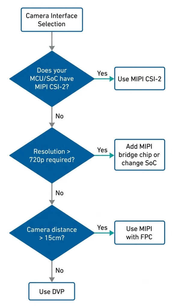
When to Use DVP and When to Use MIPI: A Decision Framework
The choice between DVP and MIPI is rarely about preference — it follows from a structured set of constraints. Work through the decision criteria below in order:
- What interface does your host SoC/MCU expose? If it only has a DVP/DCMI peripheral (STM32, ESP32), DVP is your path unless you add a bridge chip. If it has MIPI CSI-2 (Rockchip, Jetson, RPi CM4), MIPI is the path unless the sensor resolution doesn't require it.
- What resolution and frame rate does your application need? Below 720p @ 30 fps uncompressed: DVP is adequate. At 1080p or above: MIPI is required for reliable uncompressed operation. For 4K+: 2-lane MIPI minimum, 4-lane preferred.
- What is the sensor-to-host distance? If the camera module is >15 cm from the host board (e.g., remote mounting on a robot arm or inside an enclosure): DVP's skew constraints become problematic; MIPI is preferred up to 30 cm, or use a SerDes/retimer for longer runs.
- What are your software resources? If you have a small firmware team and an MCU with DCMI: DVP requires less driver complexity. If you're running Linux on an ARM SoC: V4L2 MIPI drivers are well-established and BSP support is standard; MIPI bring-up is not significantly harder than DVP in a Linux environment.
- What sensors do you need? If your application requires a specific sensor (e.g., Sony IMX415, OmniVision OV9782 for face recognition): check what interfaces that sensor supports. Most ≥3MP sensors dropped DVP support in new generations. The OV5640 is one of the few 5MP sensors still commonly available with DVP output.
Project Case — Interface Mismatch Mid-Design: "A medical device startup came to us at DVT stage with a serious problem: they had designed a patient monitoring camera around a 5MP MIPI-only sensor (Sony IMX335) on an STM32H743 MCU — a platform with no native MIPI receiver. Their previous camera vendor had not flagged this incompatibility, and they had spent three months writing firmware against a MIPI-to-parallel bridge IC that they later discovered couldn't maintain the required 30 fps throughput at 5MP due to the bridge's internal FIFO bottleneck. We proposed a pragmatic solution: downselect to OmniVision OV5640 — a 5MP sensor with a stable DVP output mode at 1080p and a well-maintained STM32 HAL driver — for the monitoring use case where 1080p at 15 fps was clinically sufficient. The OV5640 DVP module brought up on their existing PCB without any hardware changes, saving approximately $40,000 in PCB respin costs and recovering eight weeks of firmware schedule. The lesson: interface compatibility with the host platform must be verified at concept stage, not at DVT." — Smeiker Technical Sales Engineering Team
For help matching the right interface, sensor, and module configuration to your specific host platform, contact Smeiker's engineering team with your SoC model, resolution target, and application requirements.
Smeiker's DVP and MIPI Camera Module Options
Smeiker manufactures camera modules in both DVP and MIPI interfaces across a range of resolutions, sensor types, and form factors for industrial OEM integration:
- DVP camera modules: OV2640 (2MP), OV5640 (5MP), OV7670 (VGA), custom sensor options. 8-bit or 10-bit bus, 24-pin FFC connector standard. Suitable for STM32, ESP32, and FPGA-based host systems. Browse DVP camera modules →
- MIPI CSI-2 camera modules: Sony IMX415 (8MP), OmniVision OV9782 (1MP NIR), OmniVision OV4689 (4MP), IMX219 (8MP), and others. 1-lane or 2-lane configuration, 15-pin or 22-pin FPC, standard 15 cm cable. Compatible with Raspberry Pi, Rockchip, Jetson, NXP i.MX platforms. Browse MIPI camera modules →
- ODM customization: Custom FPC length, connector pinout, ISP tuning, and sensor selection for both interfaces. MOQ from 500 units. Contact our ODM engineering team with your host platform and specification.
Frequently Asked Questions
What is the main difference between DVP and MIPI camera interfaces?
DVP is a parallel interface transmitting pixel data across 8–14 simultaneous data lines. MIPI CSI-2 is a serial differential interface using 1–4 high-speed lane pairs. DVP is simpler to implement on MCUs but is bandwidth-limited to approximately 720p @ 30 fps; MIPI supports up to 4K+ at much lower pin count and better noise immunity.
Can I use a MIPI camera module with an STM32 MCU?
STM32 MCUs have a DCMI (DVP) peripheral but no native MIPI CSI-2 receiver. To use a MIPI sensor with STM32, you need a MIPI-to-parallel bridge IC. This adds PCB area, BOM cost ($2–5/unit), and firmware complexity. For STM32-based designs requiring ≥1080p, migrating to an SoC with native MIPI support (e.g., STM32MP1 or a Rockchip platform) is usually the better architectural choice.
What is the maximum resolution supported by DVP?
In practice, DVP with an 8-bit bus at 72 MHz PCLK supports 720p (1280×720) at 30 fps uncompressed. 1080p is possible with in-sensor JPEG compression (reducing data rate), but uncompressed 1080p raw output exceeds the parallel bus bandwidth for most MCU implementations. Above 3MP, most sensors only offer MIPI as their high-speed output interface.
How long can a MIPI CSI-2 FPC cable be?
Standard MIPI D-PHY FPC cables are reliable up to 20–30 cm at typical lane speeds (1.0–1.5 Gbps/lane). Beyond 30 cm, insertion loss and differential skew degrade signal integrity. Extensions up to 50–80 cm are possible with a MIPI retimer IC. For distances beyond 1 m, a SerDes solution (MIPI A-PHY, FPD-Link III, or GMSL2) is required.
Does Smeiker supply camera modules in both DVP and MIPI interfaces?
Yes. Smeiker manufactures camera modules in both DVP (8-bit, OV2640/OV5640 based) and MIPI CSI-2 (1–2 lane, Sony/OmniVision sensors, 15–22 pin FPC). Custom connector, FPC length, sensor selection, and ISP tuning are available as ODM options from 500 units. Get a free quote with your host platform and spec requirements.
Need a DVP or MIPI Camera Module for Your Design?
Tell us your host platform (MCU/SoC model), target resolution, FPC length, and annual volume. Smeiker will match you to the right module — or configure an ODM solution — with samples in 4–8 weeks.
Get a Free Quote →